Executive summary
When Ayar Labs closed its $500 million Series E in March 2026, the company stated its purpose precisely: “The company will use the funds to scale high-volume production and test capacity to accelerate the deployment of its co-packaged optics solution.” That claim, made March 3, 2026, is the claim this piece examines. The silicon works. The question is what stands between working silicon and a production accelerator in a hyperscale data center, and whether $500 million and a 2027 target are enough to close that gap.
The short answer is that the technology constraint has been largely resolved. The binding constraint is now qualification: the process by which a semiconductor optical device earns the right to sit inside a machine that a cloud operator cannot afford to have fail. That process takes longer than capital can shorten it, and the public record shows Ayar completing Engineering Validation Testing (EVT) as of August 2025, still working through Design Validation Testing (DVT), with volume-production qualification targeted for end of 2027 and customer ramps expected in 2028 to 2029.
What the money says
The $500 million Series E is, by trade coverage, the largest single funding round ever raised by a photonics company. The characterization matters less than the composition of the syndicate. NVIDIA and AMD both participated, alongside ASIC design partners MediaTek and Alchip Technologies, financial backers including ARK Invest, Insight Partners, the Qatar Investment Authority, and Sequoia Global Equities, with lead investor Neuberger Berman taking a board observer role. Neuberger Berman cited Ayar’s “execution vs. key customer milestones” as the driver of its conviction.
Two competitors investing simultaneously in the same CPO startup is not a standard term-sheet feature. It signals that both AMD and NVIDIA regard Ayar’s chiplet as infrastructure they may need regardless of whether they build their own optical interconnects, and it provides the company with strategic cover on two sides of the accelerator market. The same round that brought in sovereign wealth and growth-equity capital also brought in the companies whose silicon Ayar’s chiplet must sit beside.
Ayar Labs: Cumulative Capital Raised
As of the March close, Ayar had raised approximately $870 million across six disclosed rounds. By September 2026, a $150 million Series E extension from an undisclosed investor lifted 2026 capital raised to $650 million and the total past $1 billion. A separate $225 million secondary share purchase, led by Antero Peak Group at Artisan Partners, valued the company above $5 billion, up from $3.75 billion at the March close. Ayar has not published revenue figures, and the Series E proceeds being directed at production scaling confirms the company remains in pre-commercial-scale ramp. The record on volume has a longer spine than the Series E. On April 26, 2022, announcing the $130 million Series C, Ayar said it “made its first volume commercial shipments under contract and expects to ship thousands of units of its in-package optical interconnect by end of year,” and that the financing “allows us to fully qualify our solution against industry standards for quality and reliability and scale production starting this year.” By December 2024, the count Contrary Research reports is roughly 15,000 engineering samples. By September 2026, the target for volume-production qualification is the end of 2027. Thousands promised for 2022, fifteen thousand samples by the end of 2024, qualification at the end of 2027: each statement was accurate about the company’s intent when made, and the sequence is the measure of how long “scale production starting this year” has taken. The distinction between the ~15,000 engineering samples shipped as of December 2024 and commercial production volumes is real and material.
The technology: what is working and how
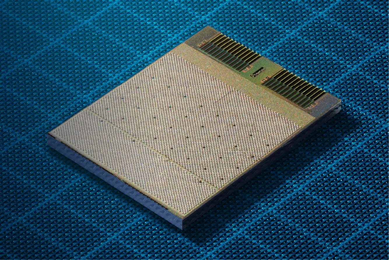
TeraPHY Gen 3, announced March 31, 2025 and detailed first in a post-deadline paper at OFC 2025 and then at Hot Chips 2025 in August, is the world’s first UCIe-compliant optical interconnect chiplet. It delivers 8 Tbps of bidirectional bandwidth across eight optical ports, each carrying 512 Gbps per direction, at sub-10 nanosecond latency and without Forward Error Correction. The doubling from the 4 Tbps second generation reflects the trajectory of a maturing product rather than a research breakthrough.
The architecture is specific and worth describing precisely, because specificity is what makes the technology claims checkable. TeraPHY uses silicon microring resonators to modulate data onto light. Each wavelength carries a 32 Gbps signal across 16 wavelengths per fiber, enabling dense wavelength-division multiplexing. The chiplet is fabricated on GlobalFoundries’ 45SPCLO 45 nm silicon-on-insulator process, a platform Ayar co-shaped. CTO Vladimir Stojanovic has described the design as portable to TSMC’s more advanced CMOS nodes, and the company is already exercising that option through the TSMC COUPE platform.
The SuperNova light source solves a problem that any co-packaged optical approach must solve: where to put the lasers. Thermally sensitive DFB lasers, supplied by Sivers Photonics, are kept remote and pluggable, away from the silicon die, in configurations supporting up to 16 wavelengths delivered into up to 16 fiber ports per module. The remote, hot-swappable design is the right engineering answer to a thermal management problem. It is also a supply-chain dependency: Ayar placed a $1 million order with Sivers Photonics in 2023 for DFB laser arrays.
TeraPHY sits at the chiplet layer of a four-tier CPO system, with the laser source kept deliberately remote
In December 2025, Alchip and Ayar demonstrated at TSMC’s European OIP Forum the first fully integrated optical connectivity solution built on TSMC’s COUPE platform: a three-chiplet subsystem consisting of an Alchip protocol-converter chiplet, an Alchip electrical integrated circuit providing SerDes and modulation drivers, and an Ayar TeraPHY photonic integrated circuit. The engine delivers up to 100 Tbps of bandwidth per accelerator. In November 2025, Global Unichip Corp announced a partnership to integrate TeraPHY into XPU multi-chip package reference designs targeting more than 200 Tbps aggregate bandwidth. In June 2026, Ayar joined the NVIDIA NVLink Fusion ecosystem, making TeraPHY optically and electrically compatible with NVIDIA’s optical and SerDes technologies.
The Wiwynn partnership, announced on March 11, 2026, extends the reference design to rack scale: a liquid-cooled architecture supporting 1,024 AI accelerators and beyond, with more than 100 Tbps of optical connectivity per accelerator and hot-swap serviceability via ELSFP light sources.
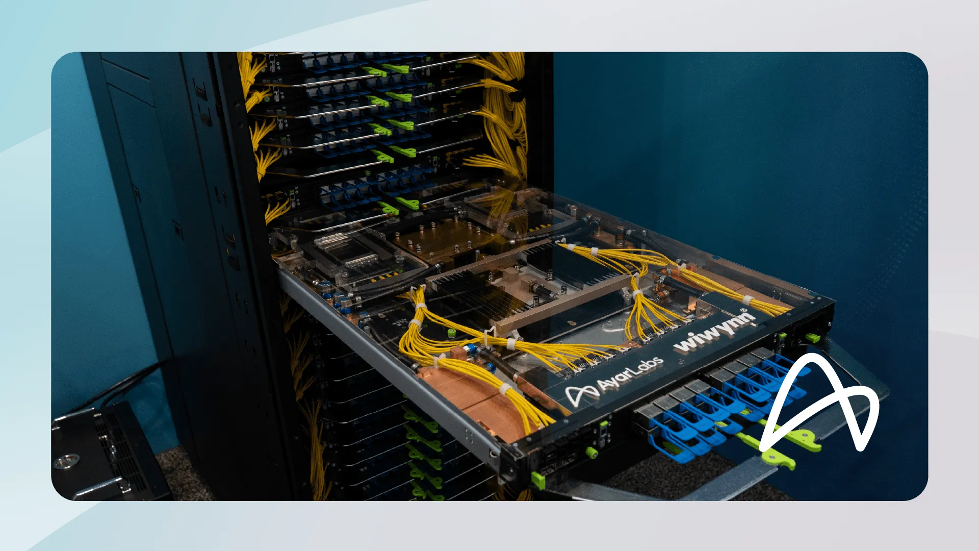
These are the integration steps a chiplet has to complete before a hyperscaler will look at it. The question is what comes after them.
The binding constraint
Qualification is the binding constraint. Not thermal management, not bandwidth, not laser supply. Qualification.
The path from working silicon to production status in a hyperscale data center has a minimum duration that money does not shorten. It runs from EVT through DVT to Production Validation Testing (PVT) and then through a customer qualification campaign that typically lasts months even when everything goes right. At each stage, a new failure mode can send the program back.
As of August 28, 2025, Ayar declared that TeraPHY Gen 3 had passed EVT “with flying colors” and was “well into DVT.” EVT results, as Ayar reports them, included temperature cycling across 30 to 80 °C with no bit-error-rate dependence on temperature, a package thermal transient that peaked near 100 °C per second, and a bench emulation in which a swept tunable laser moves the ring resonance the way a fast ramp would, which the company rates as “equivalent to temperature ramps from 160 C/s to 800 C/s.” The 800-degrees-per-second figure is Ayar’s characterization of that emulation, not a chamber cycling rate; cycling standards specify ramps per minute. The campaign also included 10-hour end-to-end link stability tests. Those are credible data points for a silicon photonics device in a demanding thermal environment. DVT completion is the next named gate before production qualification.
The reliability standard the industry reaches for is Telcordia GR-468-CORE, which covers optoelectronic device reliability for telecom equipment and requires 2,000 hours of long-term reliability testing across HTOL, damp heat, temperature cycling, THB, and ESD-HBM regimes. As iST Group analysts writing in mid-2026 noted, this standard was not designed for highly integrated co-packaged silicon photonics chiplets, and “the industry currently lacks a single, fully dedicated standard for CPO or silicon photonics products.” That absence is not a technicality. Without an agreed qualification framework, each hyperscaler runs its own campaign to its own criteria, and a chiplet that has passed one customer’s bar may need to repeat the campaign for the next.
There is a serviceability asymmetry inside the constraint that the reliability standards do not capture. A pluggable transceiver that fails is a field-replaceable unit: a technician pulls it from the faceplate and seats another in minutes, and the accelerator behind it never leaves the rack. A TeraPHY chiplet that fails is not replaceable at all. It sits inside the accelerator package, beside the XPU die, soldered to the board, and the unit of repair is the package: the accelerator itself comes out, at the cost of an XPU with its memory stacks attached. The hot-swap serviceability in the Wiwynn reference design covers the ELSFP light source, which was moved off-package precisely so that the part most likely to fail could be swapped; it does not reach the chiplet. That is why the reliability bar for a co-packaged optical engine is set by the failure cost of the package it is inside rather than by the cost of the engine, and why a hyperscaler’s qualification campaign asks a different question of a chiplet than of a transceiver.
What would have to change for this constraint to stop binding: a CPO-specific reliability standard ratified by a recognized standards body, adopted by at least one major hyperscaler as the acceptance criterion for incoming optical chiplets. That would compress the per-customer campaign into a documented compliance test. No such standard has been balloted as of mid-2026.
CTO Stojanovic, in a February 2026 interview, identified three factors that determine which CPO solutions win at scale: foundry and packaging ecosystem fit, form factor, and maturity, which he defined as “proven reliability, validated system behaviour, and a roadmap that spans generations.” His own framing places maturity, meaning qualification, as the decisive third gate, explicitly beyond silicon design. That is the clearest public statement from inside the company of what they know the problem is.
Ayar completed EVT in August 2025 and is in DVT; two further gates separate it from a production hyperscaler cluster
The team
Ayar Labs was founded in 2015 by six co-founders, all with deep academic roots in silicon photonics. The founding technology traces to a DARPA-funded collaboration, the POEM project, among MIT, UC Berkeley, and the University of Colorado in the mid-2010s, which produced a 2015 Nature paper demonstrating the world’s first processor to communicate using light. Mark Wade led the optics team on that project; it became Ayar’s founding IP.
Alex Wright-Gladstein, the founding CEO, raised the company’s first $27 million before recruiting Charles Wuischpard, a veteran of Intel and Penguin Computing, as CEO. Wade, who had served as CTO and SVP of Engineering, was appointed CEO in December 2023 after Wuischpard’s departure.
The leadership buildout since then has been deliberate. Vladimir Stojanovic was formally named CTO in January 2024 alongside two board additions: Ganesh Moorthy, then President and CEO of Microchip Technology, and Craig Barratt, former CEO of Atheros, which he sold to Qualcomm for $3.1 billion. In October 2025, Vivek Gupta joined as the company’s first Chief Strategy Officer, bringing experience from Google Cloud and Qualcomm. In February 2026, Sankara Venkateswaran joined as VP of Engineering for the TeraPHY organization, carrying 26 years of silicon engineering experience from Intel, Qualcomm, and Atheros. In June 2026, Sejal Patel Daswani joined as Chief People and Operations Officer.
The executive advisor bench includes Dan Armbrust, formerly VP of 300mm Semiconductor Operations at IBM and CEO of SEMATECH, and Rory McInerney, who spent 29 years at Intel as Corporate VP for Xeon processors across cloud, AI, HPC, and networking. Both are manufacturing-focused, which is the correct orientation for a company whose primary problem is now production rather than design.
Headcount was approximately 258 employees as of August 2026, according to Tracxn, though LeadIQ’s estimate as of July 2026 places the count in a 201-to-500 range, reflecting the imprecision typical of third-party headcount tracking for private companies. The company is actively hiring for silicon photonics validation, system validation, ASIC design verification, firmware, and photonics reliability engineering. The open roles describe the qualification campaign in job postings.
Market position and competitive pressure
The CPO market was valued at $46 million in 2024. Yole Group projects it reaches $8.1 billion by 2030, implying a 137 percent compound annual growth rate. Other forecasters put the 2030 figure higher, and the spread reflects genuine uncertainty about how quickly hyperscaler procurement shifts from pluggable transceivers to co-packaged solutions. Yole separately projects the silicon photonics transceiver market grows from $4.2 billion in 2024 to $24.8 billion by 2030.
Ayar’s primary competitive reference points are Lightmatter, which has raised approximately $850 million at a $4.4 billion valuation and whose Passage M1000 3D photonic interposer targets 114 Tbps bandwidth, and formerly Celestial AI, which Marvell acquired in early 2026 for approximately $3.25 billion in transaction value, with up to $5.5 billion in earnout milestones. Marvell expects initial Celestial revenue to begin in the second half of fiscal 2028. That timeline is instructive: an acquirer with Marvell’s manufacturing infrastructure and customer access is looking at the same 2028 ramp window that Ayar’s CEO cited to Reuters.
Lightmatter also joined NVLink Fusion and launched a 19-company Open Compute Project standardization initiative in 2026. The standardization effort is worth watching: if it produces a qualification framework that the industry adopts, it shortens the per-customer campaign for everyone, including Ayar’s competitors.
NVIDIA itself is not a passive observer. NVIDIA invested $2 billion each in Coherent and Lumentum, established photonics component suppliers, and unveiled silicon photonics switches with 1.6 Tbps ports at GTC 2025 under the Spectrum-X and Quantum-X brands. An investor that is also a vendor is a partner with a competing product road map, and Ayar’s participation in NVLink Fusion does not change that structural tension.
Ayar’s disclosed design wins include a reported order of over 5,000 units for a custom AI machine and early customer relationships with Intel (FPGA proof-of-concept) and HPE (next-generation HPC interconnect). These are engineering-sample relationships. The company projects annual shipments exceeding 100 million units by 2028, according to Contrary Research, a roughly 6,000-fold scale-up from the approximately 15,000 engineering samples shipped as of December 2024. That projection has not been confirmed by any independent source.
What would change this assessment
Two categories of evidence would increase confidence in the production timeline. First, DVT completion announced through a customer disclosure or a standards-body filing, accompanied by specific failure mode data from the thermal cycling and long-term reliability campaigns. Second, a hyperscaler qualification win announced not by Ayar but by the customer, in the form of a procurement filing, a supply agreement disclosed in an earnings call, or an import record showing optical chiplet volumes entering a data center construction project.
Two categories of evidence would reduce confidence. First, another two quarters without a DVT completion announcement would indicate the campaign found something. Second, the publication of a CPO standardization framework by Lightmatter’s OCP initiative that Ayar does not adopt or that differs materially from Ayar’s qualification approach would fragment the market into incompatible certification paths, extending the per-customer campaign.
Observables
Between now and mid-2028, four developments would move the verdict. DVT completion should produce a customer-facing data sheet or a regulatory filing from the foundry partner, either of which would appear in GlobalFoundries’ or TSMC’s public technology disclosures by mid-2027 at the latest. A hyperscaler qualification win would surface in an earnings call transcript or a supply-chain import record, both of which are public, by end of 2027. Adoption or rejection of Lightmatter’s OCP standardization initiative by a major hyperscaler would appear in OCP working group minutes, which are published, by end of 2026. And Sivers Photonics, as a publicly traded company, will disclose in its own financial filings whether the DFB laser order volumes from Ayar are growing at rates consistent with a 2027 production ramp, by mid-2027.
New research by email. Roughly one piece a month.
Sources (66)
Disclosure: the author has a social acquaintance at Ayar Labs; this piece draws only on the public record.
- AYARLABS
Ayar Labs Closes $500M Series E, Accelerates Volume Production of Co-Packaged Opticsayarlabs.com
- OPTICA-OPN
Optics & Photonics News – Ayar Labs Raises US$500 Millionoptica-opn.org
- AYARLABS
Ayar Labs, with Investments from AMD, Intel Capital, and NVIDIA, Secures $155 millionayarlabs.com
- SEMICONDUCTOR-TODAY
Ayar Labs raises $155m in Series D – Semiconductor Todaysemiconductor-today.com
- AYARLABS
Ayar Labs Raises $130 Million in Series C Fundingayarlabs.com
- BUSINESSWIRE
Ayar Labs Raises $130 Million in Series C Funding – Business Wire, April 26, 2022businesswire.com
- SEMICONDUCTOR-TODAY
Ayar Labs raises $130m in Series C – Semiconductor Todaysemiconductor-today.com
- SEMICONDUCTOR-TODAY
Ayar Labs adds $25m in expansion of $130m Series C – Semiconductor Todaysemiconductor-today.com
- SILICONCATALYST
Ayar Labs Secures $35 Million in Series B Funding – Silicon Catalystsiliconcatalyst.com
- SILICONANGLE
Co-packaged optics startup Ayar Labs raises $500M round backed by Nvidia, AMD – SiliconANGLEsiliconangle.com
- ADVENTINTERNATIONAL
Ayar Labs Secures $155 Million – Advent Internationaladventinternational.com
- CONTRARY
Ayar Labs Business Breakdown & Founding Story – Contrary Researchresearch.contrary.com
- SIVERS-SEMICONDUCTORS
Sivers Photonics receives new order worth $1m from Ayar Labs – Sivers Semiconductorssivers-semiconductors.com
- AYARLABS
Ayar Labs Unveils World's First UCIe Optical Chiplet for AI Scale-Up Architecturesayarlabs.com
- GAZETTABYTE
Ayar Labs prepares to fulfil its optical input-output (I/O) vision – Gazettabytegazettabyte.com
- CMC
GlobalFoundries Silicon Photonics GF Fotonix 45SPCLO – CMC Microsystemscmc.ca
- AYARLABS
Our SuperNova Light Source for Co-Packaged Optics – Ayar Labsayarlabs.com
- OPENCOMPUTE
Ayar Labs In-Package Optical I/O Solution – Open Compute Projectopencompute.org
- BUSINESSWIRE
Ayar Labs Demonstrates Industry's First 4-Tbps Optical Solution – Business Wirebusinesswire.com
- AYARLABS
TeraPHY Optical I/O Chiplet – Ayar Labsayarlabs.com
- SERVETHEHOME
Ayar Labs UCIe Optical IO Retimer at Hot Chips 2025 – ServeTheHomeservethehome.com
- LIGHTCOUNTING
September 2025 Hot Conferences Feature Cool Optics – LightCountinglightcounting.com
- TOMSHARDWARE
Industry's first TSMC COUPE-based optical connectivity solution – Tom's Hardwaretomshardware.com
- PICMAGAZINE
Alchip and Ayar Labs debut first TSMC COUPE-based optical connectivity engine – PIC Magazinepicmagazine.net
- GUC-ASIC
GUC and Ayar Labs Partner to Advance Co-Packaged Optics – GUCguc-asic.com
- THEREGISTER
Ayar Labs eyes hyperscale customers with GUC design collab – The Registertheregister.com
- WIWYNN
Ayar Labs and Wiwynn Partner to Bring Co-Packaged Optics to Rack-Scale AI Systems – Wiwynnwiwynn.com
- DATACENTERDYNAMICS
Ayar Labs and Wiwynn partner for development of co-packaged optical AI infrastructure – Data Centre Dynamicsdatacenterdynamics.com
- ERICSSON
GR-468-CORE, Generic Reliability Assurance Requirements for Optoelectronic Devices Used in Telecommunications Equipment – Telcordiatelecom-info.njdepot.ericsson.net
- ISTGROUP
Can Legacy GR-468 Handle SiPh & CPO? – iST Groupistgroup.com
- OPENLIGHTPHOTONICS
OpenLight Achieves Successful Completion of Telcordia GR-468 Qualificationopenlightphotonics.com
- BUSINESSWIRE
Ayar Labs Strengthens Leadership Team and Expands Global Presence – Business Wirebusinesswire.com
- DATACENTERDYNAMICS
Optical interconnect startup Ayar Labs closes $500m funding round – Data Centre Dynamicsdatacenterdynamics.com
- AYARLABS
Leadership Team – Ayar Labsayarlabs.com
- AYARLABS
Ayar Labs Names Mark Wade CEOayarlabs.com
- HPCWIRE
Optical I/O Pioneer Tapped for Ayar Labs CEO Position – HPCwirehpcwire.com
- SEMICONDUCTOR-TODAY
Ayar Labs names co-founder & CTO Mark Wade as CEO – Semiconductor Todaysemiconductor-today.com
- SEMICONDUCTOR-TODAY
Ayar Labs' board gains silicon industry veterans – Semiconductor Todaysemiconductor-today.com
- LIGHTWAVEONLINE
Ayar Labs adds two to board of directors, names new CTO – Lightwavelightwaveonline.com
- AYARLABS
Ayar Labs Appoints Vivek Gupta as Chief Strategy Officerayarlabs.com
- COMPOUNDSEMICONDUCTOR
Ayar Labs appoints chief strategy officer – Compound Semiconductorcompoundsemiconductor.net
- AYARLABS
Ayar Labs Names Sankara Venkateswaran as Vice President of Engineeringayarlabs.com
- SEMICONDUCTOR-TODAY
Ayar Labs names Sankara Venkateswaran as VP of engineering – Semiconductor Todaysemiconductor-today.com
- LEADIQ
Ayar Labs Employee Directory – LeadIQleadiq.com
- TRACXN
- YOLEGROUP
Co-Packaged Optics for Data Centers 2025 – Yole Groupyolegroup.com
- YOLEGROUP
Co-Packaged Optics: Powering the Next Wave of AI Infrastructures – Yole Groupyolegroup.com
- YOLEGROUP
Silicon Photonics and Co-Packaged Optics at the Heart of Next-Generation AI-Driven Data Infrastructure – Yole Groupyolegroup.com
- AYARLABS
Ayar Labs Joins NVIDIA NVLink Fusion Ecosystemayarlabs.com
- MARVELL
Marvell Completes Acquisition of Celestial AIinvestor.marvell.com
- SEC
- SEMIANALYSIS
Co-Packaged Optics (CPO) – Scaling with Light – SemiAnalysisnewsletter.semianalysis.com
- LIGHTMATTER
Lightmatter Raises $400M Series D; Quadruples Valuation to $4.4B – Lightmatterlightmatter.co
- DATACENTERDYNAMICS
Lightmatter launches 19-company initiative to standardize silicon photonics-ready infrastructure – Data Center Dynamicsdatacenterdynamics.com
- SUBSTACK
Ayar Labs | Co-packaged Optics Revolution – SemiAnalysissemianalysis.substack.com
- NVIDIA
NVIDIA and Coherent Announce Strategic Partnership to Develop Optics Technology – NVIDIA Newsroomnvidianews.nvidia.com
- NVIDIA
NVIDIA Announces Strategic Partnership With Lumentum to Develop State-of-the-Art Optics Technology – NVIDIA Newsroomnvidianews.nvidia.com
- AYARLABS
Let's Get Serious: TeraPHY Optical Engine Passes the Test for AI Scale-Up at Volume – Ayar Labsayarlabs.com
- SILICONANGLE
Ayar Labs bags $150M in additional Series E funding – SiliconANGLEsiliconangle.com
- REUTERS
Ayar Labs backed by chip giants extends funding round by $150 million – Reutersreuters.com
- SEMICONDUCTOR-TODAY
Ayar Labs expands 2026 funding to $650m – Semiconductor Todaysemiconductor-today.com
- LIGHTWAVEONLINE
Ayar Labs scales funding to $650M – Lightwavelightwaveonline.com
- PHOTONICS
Ayar Labs Secures $155M from Investors Including AMD, NVIDIA – Photonics Spectraphotonics.com
- OPTICA-OPN
Ayar Labs Gets Key Funds from Chip Giants – Optics & Photonics Newsoptica-opn.org
- OPTICALCONNECTIONSNEWS
OFC 2025: Ayar Labs first UCIe with optical chiplet for AI scale-up – Optical Connections Newsopticalconnectionsnews.com
- WELLFOUND
Jobs at Ayar Labs – Wellfoundwellfound.com